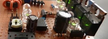
A thumbnail-size microcontroller controlling a 70-watt audio amplifier sounds like the beginning of an electronics joke. The punchline is that it actually worksalthough the tiny chip is not personally shoving 70 watts into a speaker like a very determined ant carrying a refrigerator.
The ATtiny45 acts as the amplifier’s signal-processing brain. It samples an analog audio input, converts that signal into pulse-width modulation, and controls an external MOSFET power stage. The transistors, power supply, bridge circuit, and output filter handle the muscle work. Together, they create a minimalist Class-D amplifier that is far more educational than its short parts list suggests.
This project is not a modern plug-and-play audiophile amplifier. It lacks the feedback, protection systems, precision converters, and polished specifications found in commercial Class-D chips. What it offers instead is a wonderfully direct lesson in PWM audio, MOSFET switching, H-bridge operation, filtering, firmware timing, and the creative abuse of inexpensive microcontrollers.
What Is the 70 Watt ATtiny Amplifier?
The original design was created by electronics hobbyist Rouslan Dimitrov around an ATtiny45, an eight-bit AVR microcontroller. The amplifier ran from a 12-volt supply and used a bridged MOSFET output stage rather than asking the microcontroller’s tiny I/O pins to drive a loudspeaker directly.
That distinction matters. An ATtiny pin can deliver only a small amount of current. Connect a large speaker directly to it, and the loudest sound may be the microcontroller quietly entering the afterlife. In this design, the ATtiny produces carefully timed control signals, while external power MOSFETs switch the much larger current required by the speaker.
The first version used the ATtiny’s built-in analog-to-digital converter and an eight-bit timer to generate two PWM outputs. A later revision improved low-volume performance by taking advantage of the chip’s high-speed timer, 64 MHz phase-locked loop clock, double-buffered compare registers, and carefully written interrupt code.
The result is a mono Class-D amplifier assembled from a surprisingly small group of parts: the ATtiny, several MOSFETs, biasing components, power-supply capacitors, an input network, and an LC output filter.
How a Class-D Amplifier Turns Pulses Into Music
A traditional linear amplifier asks its output transistors to operate partly on, partly off, and everywhere in between. That approach can produce excellent audio, but the transistors often dissipate substantial energy as heat.
A Class-D amplifier treats the output transistors more like switches. Ideally, each MOSFET is either fully on or fully off. When it is off, almost no current passes through it. When it is fully on, the voltage drop across it is small. Less simultaneous voltage and current means less wasted power and less heat.
Pulse-width modulation carries the audio
The amplifier represents the changing audio voltage as a rapidly switching digital waveform. The width of each pulse changes according to the instantaneous audio level.
A signal near the center level produces roughly equal high and low periods. A positive audio excursion increases the pulse width in one direction. A negative excursion reduces it or increases the complementary output. The waveform looks like an energetic square-wave fence, but its average value follows the original music.
The output filter removes the switching carrier
The speaker should receive the audio content, not the raw high-frequency switching waveform. An LC low-pass filter uses an inductor and capacitor to suppress much of the PWM carrier while allowing audible frequencies to pass.
The speaker’s voice coil also contributes inductance, but relying entirely on the speaker is not ideal in a higher-power experimental amplifier. A properly designed output filter reduces switching noise, limits unwanted heating, and helps control electromagnetic interference.
The H-bridge increases voltage swing
The ATtiny amplifier uses a bridged output arrangement. Instead of holding one speaker terminal at ground and moving only the other, the circuit drives both sides in opposite directions.
When one side of the bridge rises, the other falls. This produces a larger differential voltage across the speaker from the same supply. Bridge-tied-load operation is common in automotive and portable audio because it extracts more useful output from a limited supply voltage.
The Signal Path From Audio Jack to Speaker
1. Input coupling and level adjustment
The incoming line-level audio signal first passes through coupling and bias components. Audio sources normally swing above and below zero volts, but the ATtiny’s ADC cannot safely measure negative voltage. The circuit shifts the signal into the ADC’s permitted input range.
A potentiometer or resistor network adjusts the input level. This stage is important because too little signal wastes available resolution, while too much drives the ADC into clipping. Once clipping begins, the output stops resembling music and starts resembling a square wave with anger-management issues.
2. Analog-to-digital conversion
The ATtiny45 contains a 10-bit ADC. It repeatedly samples the conditioned audio waveform and produces numerical values representing the input voltage.
Although the ADC offers 10-bit results, the basic PWM hardware is only eight bits. That mismatch creates a challenge: how can the circuit preserve more information than a single PWM period can represent?
3. Firmware extends effective PWM precision
The second revision uses consecutive timer cycles to distribute a higher-resolution value over time. When the desired output exceeds what one eight-bit cycle can hold, the software places part of the value in one cycle and the remainder in the next.
The audio system, output filter, and human ear average these rapidly alternating values. This technique allows the design to approach nine-bitand under certain conditions even greatereffective precision in the audible range without replacing the microcontroller.
The first revision used dithering and intentionally asymmetrical PWM signals to improve low-level sound. The later version no longer required the same dithering method because the multi-cycle PWM approach handled quiet passages more gracefully.
4. Complementary bridge control
Two PWM channels control opposite halves of the H-bridge. In the improved strategy, both sides operate near 50% duty cycle when the audio input is centered. Because the bridge outputs move together at idle, the differential voltage across the speaker remains close to zero.
This approach consumes slightly more switching energy than keeping one side inactive, but it improves reproduction of very small signals. The alternative zero-duty strategy created extremely short pulses at low levels, and the real MOSFETs could not switch quickly enough to reproduce them accurately.
5. MOSFET power conversion
The PWM outputs control external N-channel and P-channel MOSFETs. These devices connect the speaker circuit alternately to the power rails.
MOSFET selection involves more than choosing the lowest advertised on-resistance. Gate charge, capacitance, switching speed, voltage rating, current rating, body-diode behavior, and available gate-drive voltage all affect performance. A transistor that looks heroic in a catalog may become a pocket-size space heater when switched inefficiently.
Why the ATtiny45 Is Surprisingly Suitable
The ATtiny45 was not marketed as a dedicated digital audio processor. Nevertheless, it contains several peripherals that happen to fit this experiment remarkably well.
- A 10-bit ADC can sample an analog audio input.
- Two high-frequency PWM outputs can drive complementary bridge signals.
- A high-speed timer can run from an internal PLL clock.
- Timer interrupts allow precise, cycle-by-cycle output updates.
- Programmable dead-time features help prevent dangerous switching overlap.
- The small package keeps the control circuit inexpensive and compact.
The real achievement is not simply selecting the chip. It is using the hardware peripherals efficiently enough that the CPU does not need to calculate every waveform transition manually. The timer, ADC, and compare registers perform much of the repetitive work, while the firmware mainly moves data at exactly the right moment.
Does This Amplifier Really Produce 70 Watts?
The “70 watt” label needs context. It should not be treated as a laboratory-certified continuous RMS rating with a specified distortion level.
The original project described a 12-volt bridged amplifier and connected the 70-watt figure partly to the current capability of the MOSFETs. A 6-amp current through a 2-ohm load corresponds to P = I²R = 6² × 2 = 72 watts. Electrically, that calculation is valid for the stated current, but it does not prove that the amplifier delivers a clean 72-watt sine wave continuously.
Supply voltage sets another hard limit. An ideal full bridge powered by 12 volts can place approximately a plus-or-minus 12-volt waveform across the load. For a sine wave, the theoretical maximum power is approximately:
P = V² / (2R)
Using a 12-volt supply, that works out to about 18 watts into 4 ohms or 36 watts into 2 ohms, before accounting for transistor losses, filter resistance, supply sag, and distortion.
A full-amplitude square wave across 2 ohms could approach 72 watts because its RMS voltage equals its peak voltage. Unfortunately, a full-scale square wave is better suited to testing speaker warranties than enjoying music.
The fairest interpretation is that the circuit can control a power stage operating in the tens-of-watts range, while the exact clean output depends on the power supply, load impedance, cooling, filter, MOSFETs, waveform, and acceptable distortion. The ATtiny does not establish the wattage; the surrounding power electronics do.
Advantages of the Minimalist ATtiny Amplifier
- Low component count: The microcontroller replaces a separate oscillator, PWM comparator, and portions of the control circuitry.
- High educational value: One project demonstrates ADC sampling, timers, interrupts, PWM, gate control, filters, and power electronics.
- Firmware flexibility: Modulation behavior can be changed without redesigning the entire analog control circuit.
- Good efficiency: Properly switched MOSFETs dissipate less heat than comparable linear output stages.
- Compact construction: The controller itself occupies very little board space.
- Low cost: The core electronics can be assembled from inexpensive, commonly understood components.
Limitations That Matter in Real Use
Limited resolution
Eight- and ten-bit signal paths are suitable for experimentation, alarms, compact speakers, effects, and casual listening, but they are not equivalent to a modern 16-, 24-, or 32-bit audio chain. Quantization becomes especially noticeable at low volume unless the firmware uses noise shaping, dithering, oversampling, or multi-cycle PWM techniques.
No global feedback loop
The original circuit operates without measuring the final speaker output and correcting errors. That keeps the design simple, but distortion from the MOSFETs, power supply, timing, filter, and load remains largely uncorrected.
In a feedback-based amplifier, the controller compares the actual output with the desired signal and continually reduces the difference. Adding that feature to a microcontroller design is possible, but it demands more ADC performance, processing time, careful loop compensation, and protection against instability.
Power-supply noise
The output stage switches the supply directly, so noise or sag on that rail can appear in the audio. Large local decoupling capacitors, short current paths, a low-impedance supply, and sensible grounding are essential.
Shoot-through risk
If the high-side and low-side MOSFETs in one bridge leg turn on simultaneously, they create a near-direct short across the supply. This condition is called shoot-through, and it can destroy transistors faster than someone can say, “Why is the bench supply clicking?”
Dead time, gate clamps, suitable drivers, and verified switching waveforms are therefore critical. The original design used LEDs as improvised zener-like clamps, while a later update replaced them with actual zener diodes and adjusted component values to improve switching.
EMI and layout sensitivity
Fast switching edges contain high-frequency energy. Long wires, large current loops, poor grounding, and a casually routed output filter can create ringing, radio interference, and mysterious noise.
A solderless breadboard is convenient for slow logic experiments but poorly suited to a high-current Class-D output stage. A compact PCB or carefully constructed perfboard layout is much more reliable.
Missing commercial protection features
Modern amplifier ICs commonly include overcurrent shutdown, thermal protection, undervoltage lockout, DC detection, controlled startup, muting, and short-circuit protection. A minimalist ATtiny amplifier needs these protections added separately if it will be used beyond supervised experimentation.
Practical Building and Testing Checklist
- Program and verify the ATtiny before connecting the power MOSFET stage.
- Confirm the PLL, timer mode, PWM frequency, fuse settings, and ADC reference configuration.
- Inspect both PWM outputs with an oscilloscope and verify that they behave correctly at idle.
- Check dead time before applying full supply voltage.
- Begin with a current-limited bench supply at a reduced voltage.
- Use a noninductive power resistor as a dummy load before connecting an expensive speaker.
- Monitor MOSFET and inductor temperature during low-power tests.
- Measure for DC voltage across the output before attaching a speaker.
- Keep the bridge, supply capacitors, and filter physically close together.
- Increase input level and supply voltage gradually while watching the output waveform for clipping or ringing.
A passive guitar pickup or microphone will usually need a preamplifier. The ATtiny circuit expects a suitably conditioned audio signal; it is a power amplifier controller, not a complete studio channel strip wearing a tiny eight-pin disguise.
Hands-On Experiences With an ATtiny Class-D Amplifier
A realistic ATtiny amplifier build rarely begins with glorious music. It usually begins with silence, one suspiciously warm transistor, and several minutes of staring at fuse-bit settings.
The first major lesson is that firmware configuration matters as much as soldering. The high-speed timer depends on the correct PLL and clock setup. When the chip runs from the wrong clock source, the PWM carrier may fall into or near the audible range. Instead of music, the speaker may produce a whistle that sounds like a tea kettle applying for a job in cybersecurity.
Builders also discover that substitute MOSFETs are not automatically equivalent. A replacement may have a lower on-resistance yet still run hotter because its gate capacitance is larger and the control circuit cannot charge or discharge it quickly. The transistor then spends more time in the partially conducting region, where voltage and current overlap and create heat.
Another common experience is that the amplifier sounds acceptable at moderate volume but becomes rough near clipping. This behavior is not surprising. The ADC has finite input range, the PWM has limited resolution, and there is no global feedback loop correcting the final output. Once the input reaches the numerical limits, the firmware cannot request a wider pulse. The tops of the waveform flatten, high-frequency harmonics increase, and the speaker begins announcing that mathematics has reached the edge of the map.
Low-volume listening reveals a different problem. With ordinary eight-bit PWM, quiet audio occupies only a small number of available output steps. Voices and fading notes can sound grainy or disappear. The revised multi-cycle technique improves this by distributing fractional output values across consecutive PWM periods. Hearing that improvement is a useful demonstration of how oversampling, averaging, and noise shaping can increase perceived resolution without changing the physical timer width.
Power-supply quality is another bench lesson that arrives quickly. The amplifier may operate cleanly from a regulated supply but hum or buzz when powered from a noisy adapter. Because the bridge switches the supply rail into the output network, poor decoupling and ground layout can make power-supply artifacts audible. Adding local bulk capacitance, a small ceramic bypass capacitor near the controller, and shorter current paths often produces a surprisingly large improvement.
The LC filter deserves equal respect. An inductor with excessive winding resistance reduces output power and becomes warm. A poorly selected capacitor can carry more high-frequency current than expected. Long filter wiring encourages ringing. Builders who initially treat the filter as an optional finishing touch often learn that it is a central part of the amplifier, not decorative electronic parsley.
Testing with a dummy load rather than a speaker is one of the most valuable habits. A power resistor does not care about brief whistles, DC offsets, or experimental waveforms. It allows voltage, current, frequency, and heating to be measured without risking a woofer. Once the output is stable, the speaker can be connected at low volume and the input increased carefully.
The most rewarding experience is seeing a recognizable audio waveform emerge from a circuit controlled by such a modest microcontroller. The ATtiny45 is not performing advanced digital signal processing. It is repeatedly sampling, updating timer registers, and maintaining precise timing. Yet those simple actions are enough to control a genuine power stage.
That is why the project remains memorable. A commercial Class-D module is easier, quieter, safer, and usually better. The ATtiny amplifier, however, exposes the machinery. Every buzz suggests a grounding problem. Every hot MOSFET points toward switching loss. Every low-volume artifact reveals the cost of limited resolution. It turns audio amplification from a mysterious black box into a set of visible engineering trade-offs.
Conclusion
The 70 Watt Amp Uses An ATtiny project is best understood as an inventive microcontroller-controlled Class-D experiment rather than a finished high-fidelity product. Its tiny AVR samples analog audio, creates complementary PWM signals, and directs an external MOSFET bridge that supplies the actual speaker power.
The design demonstrates how much can be achieved with limited hardware when timers, ADCs, interrupts, and firmware are used creatively. It also exposes the less glamorous realities of power electronics: dead time, filtering, gate charge, supply noise, output-power math, EMI, and the occasional transistor attempting to become a toaster.
For builders who want a dependable everyday amplifier, a modern integrated Class-D device is the practical choice. For anyone who wants to understand what happens inside that device, the ATtiny amplifier remains a fascinating project.