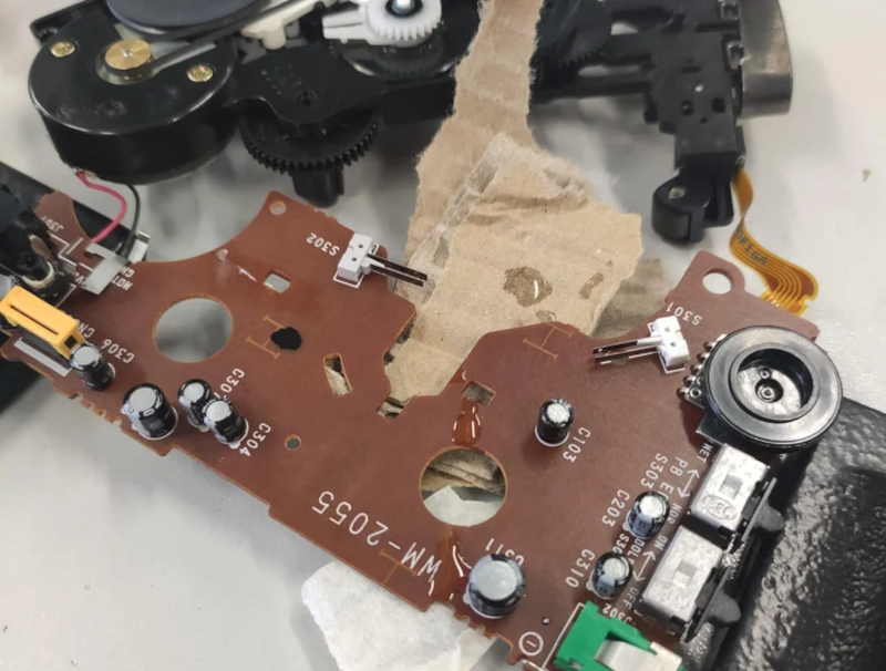
PCB repair is one of those jobs that looks simple right up until the copper pad leaves the board like it has somewhere better to be. One minute you are calmly replacing a connector; the next, you are staring at a lifted trace, a shiny blob of solder, and the quiet realization that printed circuit boards have feelingsand apparently, very delicate skin.
The “sticky” part of PCB repair is not just about solder paste, flux, epoxy, UV solder mask, conformal coating, or the occasional bit of adhesive-backed copper. It is also about decision-making. Should you rebuild the pad? Run a jumper wire? Scrape back the solder mask? Replace the board entirely? A good repair is not merely a heroic act with a soldering iron. It is diagnosis, restraint, cleanliness, temperature control, and a tiny bit of humility served under magnification.
Whether you are restoring vintage electronics, fixing a gaming console, repairing an industrial controller, or saving a prototype from the recycling bin, successful circuit board repair depends on understanding what failed, why it failed, and how to restore both electrical continuity and mechanical strength. In other words, you are not just making electrons move again. You are persuading a wounded board to trust you.
What Makes PCB Repair So Tricky?
A printed circuit board is a layered structure. Copper traces carry signals and power, solder mask protects the copper, pads provide attachment points for components, and the fiberglass substrate gives the whole thing strength. When everything is healthy, it is a tiny city of electrical roads. When heat, force, corrosion, or poor handling gets involved, that city starts developing potholes.
The most common PCB repair problems include lifted solder pads, broken traces, cracked solder joints, damaged vias, solder bridges, burned areas, corrosion, and missing mask. Each issue requires a different repair strategy. A lifted pad that still connects to a trace may be saved with epoxy and careful soldering. A missing pad may need a replacement copper land or a jumper wire. A broken trace may require scraping back solder mask, tinning exposed copper, and bridging the gap with fine wire.
The challenge is that PCBs do not forgive rough work. Too much heat can delaminate copper. Too much pressure can tear traces. Too much solder can bridge neighboring pins. Too little cleaning can leave residues that cause future trouble. PCB repair is sticky because every fix must attach, conduct, insulate, and survive vibration, heat cycles, and normal use.
The First Rule: Diagnose Before You Touch the Iron
The best PCB repair begins with doing absolutely nothing for a minute. That may feel unproductive, but it beats confidently making the problem worse. Start by inspecting the board under good lighting and magnification. Look for lifted copper, darkened laminate, cracked joints, missing components, green or white corrosion, loose connectors, and signs of previous repair attempts.
A multimeter in continuity mode is your best friend here. Use it to confirm where a pad or trace should connect. Do not assume the nearest shiny copper is the correct destination. On modern boards, traces may disappear into vias, travel through inner layers, or connect to components on the other side. A schematic, board view, or known-good reference board can save you from creating a jumper wire that proudly connects two things that were never supposed to meet.
Also check whether the board is worth repairing. A single broken trace on a low-voltage control board is usually reasonable. A charred multilayer power board with internal damage is a different story. Good repair work includes knowing when to stop. The soldering iron is a tool, not a magic wand with a hot metal nose.
Cleanliness Is Not Optional
PCB repair loves clean surfaces. Dirt, oil, oxidation, old flux, and corrosion all make soldering harder. Before repairing a damaged pad or trace, clean the area with appropriate electronics-safe cleaner, such as high-purity isopropyl alcohol, and allow it to dry fully. Remove loose debris, burned mask, and flaky copper carefully.
Flux is another key player. Flux helps solder wet the copper instead of forming dull blobs that behave like tiny metallic cats refusing to sit where you want them. Use the right amount: enough to promote flow, not so much that the board looks like it has been glazed for a pastry competition. After soldering, clean remaining flux residue when needed, especially around high-impedance circuits, connectors, and fine-pitch components.
Temperature Control: Hot Enough, Not Barbaric
Many PCB repair disasters begin with the phrase, “I’ll just turn the iron up a little.” Heat is necessary, but uncontrolled heat is how pads lift, solder mask bubbles, and plastic connectors become modern art. A temperature-controlled soldering station is strongly recommended. The goal is to heat the joint efficiently, complete the work quickly, and leave the surrounding board as relaxed as possible.
Large ground planes, lead-free solder, thick copper, and multilayer boards often require more thermal energy than small hobby boards. In those cases, preheating the board can reduce thermal shock and make rework safer. Professional rework systems use controlled airflow, preheaters, board supports, and temperature monitoring because the board is not just a flat objectit expands, flexes, and stores heat unevenly.
For hand repair, use the correct tip size. A needle tip may seem precise, but if it cannot transfer enough heat, you will keep it on the joint too long and increase the risk of damage. A slightly larger, clean, well-tinned tip often performs better because it transfers heat quickly.
Repairing Lifted Pads
A lifted pad happens when the copper land separates from the board. This can occur during desoldering, connector removal, excessive heat, mechanical stress, or a moment of impatience that future-you will remember vividly.
When the Pad Is Still Present
If the pad is lifted but still intact, do not keep bending it like you are testing a paperclip. Clean underneath it, place a small amount of suitable epoxy under the lifted copper, press it back into position, and let it cure according to the adhesive instructions. After the pad is mechanically secure, restore soldering only with minimal heat and support the repaired area where possible.
This method works best when the pad still has a valid electrical connection and the component does not place heavy mechanical stress on it. For connectors, switches, and sockets, the repair may need reinforcement because those parts get pulled, pushed, plugged, and abused by everyday life.
When the Pad Is Gone
If the pad is missing, you have two common options: replace the pad with a copper repair land or bypass it with a jumper wire. A replacement land can be bonded to the board using epoxy, then connected to the original trace. A jumper wire can connect the component lead directly to the next valid electrical point in the circuit.
Fine enameled wire, often called magnet wire, is popular for this work because it can route through tight spaces. The wire should be secured with UV solder mask, epoxy, or another suitable coating so it does not move and fatigue the joint. A loose jumper wire is not a repair; it is a future mystery failure wearing a disguise.
Repairing Broken PCB Traces
A broken trace interrupts the electrical path. The repair goal is simple: restore continuity without creating shorts or weakening the board further. First, identify both ends of the damaged connection. Then gently scrape the solder mask from healthy copper on each side of the break. Tin the exposed copper with flux and solder. Bridge the gap with fine wire or a copper repair strip, then secure and insulate the repair.
Do not scrape more than necessary. The copper on many boards is thin, and aggressive scraping can turn a repairable trace into confetti. After soldering, inspect the joint under magnification and test continuity. Also test for shorts to nearby traces. A repaired trace should conduct where it should and absolutely not conduct where it should not. Electronics are picky like that.
Solder Bridges, Cold Joints, and Other Sticky Surprises
A solder bridge occurs when solder connects two adjacent pads or pins unintentionally. It is especially common on fine-pitch ICs and connectors. The fix usually involves flux, a clean iron tip, and desoldering braid. Place the braid over the bridge, heat it through the braid, and let it absorb excess solder. Lift the braid and iron together to avoid soldering the braid to the board and accidentally pulling up a pad.
Cold joints are another frequent issue. They may look dull, cracked, lumpy, or poorly wetted. A cold joint can cause intermittent problems that appear only when the device warms up, vibrates, or decides to ruin your afternoon. Reflowing the joint with flux and proper heat often solves the issue, but recurring cold joints may indicate mechanical stress, contamination, or an underlying component problem.
Adhesives, Epoxy, and UV Solder Mask
This is where the “sticky proposition” becomes literal. PCB repair often needs adhesives because solder alone is not structural glue. Solder makes an electrical and metallurgical connection; it should not be expected to hold a torn pad to fiberglass forever. For lifted conductors, replacement pads, and secured jumper wires, epoxy or UV-curable solder mask can provide mechanical support and insulation.
UV solder mask is useful for small repairs because it cures quickly under UV light and can hold fine wires in place. Epoxy is often stronger but may require careful mixing, accurate placement, and cure time. The key is to keep adhesive away from surfaces that must be soldered later. Once adhesive contaminates a pad, soldering becomes far less cooperative.
Conformal coating adds another layer to the repair story. Some boards are coated for moisture, dust, or chemical protection. Before soldering, coating must be removed from the repair area. After the repair, the protective coating may need to be restored. A board used in a humid garage, appliance, vehicle, or industrial environment should not be left with bare copper exposed unless you enjoy corrosion as a hobby.
ESD Safety and Handling
Electrostatic discharge can damage sensitive components even when you do not feel a spark. Use an ESD-safe mat, wrist strap, and proper storage bags when handling vulnerable boards. Avoid shuffling across carpet with a naked motherboard in your hand like a villain in a low-budget electronics drama.
Also disconnect power before repair. Remove batteries when possible, and be especially cautious with boards connected to high-voltage power supplies, capacitors, or lithium battery packs. If a board stores dangerous energy or belongs to safety-critical equipment, professional repair is the smarter path.
When a Jumper Wire Is Better Than a Perfect-Looking Pad
Beginners often want the repair to look exactly like the original board. That is understandable, but the best repair is the one that is electrically correct, mechanically secure, and reliable. Sometimes a neat jumper wire is better than an ornamental pad reconstruction that looks impressive but fails after three connector insertions.
For signal lines, jumper wires are often practical. For high-current paths, high-frequency signals, controlled-impedance traces, RF circuits, and power electronics, the repair must be more carefully evaluated. Wire length, routing, gauge, insulation, and proximity to other signals can matter. A jumper that works on a keyboard matrix may not be acceptable on a high-speed USB data line or a motor driver output.
Practical PCB Repair Workflow
A reliable workflow keeps the repair calm and repeatable. Start by documenting the damage with photos. Clean the board. Inspect under magnification. Map the circuit with a meter. Decide whether the repair needs a pad rebuild, trace bridge, jumper, component replacement, or board replacement. Prepare the surface. Use flux. Apply controlled heat. Secure the repair mechanically. Clean again. Inspect again. Test continuity and shorts. Then power the board carefully, preferably with current limiting when appropriate.
This sounds slow, but it is faster than repairing the repair. Most PCB mistakes happen when the technician skips inspection, rushes the desoldering, or uses the soldering iron as a pry bar. A soldering iron should melt solder, not negotiate with parts by force.
Common Mistakes That Ruin PCB Repairs
Using Too Much Force
If a component does not move, the solder is not fully molten or all pins are not free. Pulling harder usually removes copper, not the component. Add flux, use the correct desoldering method, and be patient.
Overheating the Board
Repeated long heat cycles can lift pads and weaken adhesives inside the board. Use enough heat to work efficiently, but avoid cooking the area.
Skipping Mechanical Reinforcement
A tiny wire soldered to a trace may pass a continuity test but fail later if it moves. Secure jumper wires and rebuilt pads with suitable coating or adhesive.
Ignoring the Root Cause
If a connector ripped off because the cable is under tension, replacing the connector without strain relief simply schedules the next failure. Repair the cause, not just the symptom.
Experience Notes: Lessons From the Sticky Side of PCB Repair
Anyone who has repaired more than a few PCBs eventually develops a private museum of mistakes. There is the board where the pad lifted because the desoldering braid was yanked sideways. There is the connector that looked perfectly aligned until magnification revealed one rebellious pin floating in the air. There is the “quick reflow” that became a half-hour rescue mission because the board had a giant ground plane drinking heat like iced tea in July.
One of the biggest lessons is that preparation beats bravery. A clean bench, stable board holder, good lighting, and magnification make the repair feel less like surgery performed in a moving taxi. Before touching the iron, it helps to anchor the board so both hands are free. One hand can manage the iron, the other can guide solder, tweezers, wick, or wire. Trying to hold the board with your wrist while soldering with two fingers is how heroic legends begin, and not the good kind.
Another lesson is that flux is not cheating. Many ugly joints are not caused by lack of skill but by oxidation, contamination, or poor heat transfer. A small amount of quality flux can turn a stubborn joint into a cooperative one. The difference feels almost unfair, like discovering the board had a “please behave” button all along.
Patience is equally important when repairing lifted pads. The temptation is to solder first and stabilize later, but fragile copper needs support. If a pad is already moving, every additional heat cycle and touch can make it worse. Securing it with epoxy or replacing the electrical path with a properly routed jumper often produces a stronger result than trying to pretend the damage never happened.
Testing also deserves respect. A continuity beep is useful, but it is not the whole story. After repairing a broken trace, check the intended connection and nearby pads. Shorts can hide under flux residue, between fine-pitch pins, or beside a jumper wire that shifted slightly before the mask cured. Visual inspection under magnification catches what confidence misses.
Experience also teaches when not to chase beauty. A factory PCB trace is elegant, but a repair does not have to win a design award. It needs to be correct, insulated, supported, and serviceable. A clean jumper wire secured with solder mask may look like a tiny green railroad, but if it restores the circuit safely, it has done its job.
The final lesson is emotional: walk away before frustration takes the wheel. PCB repair rewards calm hands. When the solder will not flow, the wick sticks, or the pad starts to curl, stop and reassess. Clean the area, change the tip, add flux, lower the temperature, raise the temperature, preheat the board, or practice on scrap. The board is not mocking you. Probably. But it will absolutely punish rushing.
Conclusion
PCB repair is a sticky proposition because it combines electrical troubleshooting, surface preparation, soldering skill, adhesive technique, and judgment. The repair must conduct electricity, survive handling, avoid shorts, and protect exposed copper. That is a lot to ask from a space smaller than a grain of rice.
The good news is that most common PCB problems are manageable when approached carefully. Diagnose first, clean thoroughly, control heat, use flux wisely, reinforce fragile areas, and test everything before declaring victory. Whether you are rebuilding a lifted pad, bridging a broken trace, clearing a solder bridge, or securing a jumper wire, the goal is not just to make the board work today. The goal is to make it keep working tomorrow, after the case is closed and the tiny repair is out there living its best electronic life.